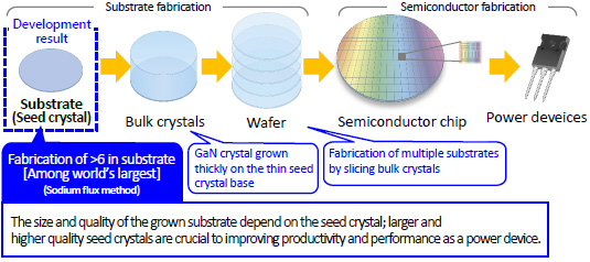
Power devices are widely used for power control in industrial machinery, automobiles, home electronics and more. As society moves toward carbon neutrality, the practical application and widespread use of next-generation power devices is promising as a means of reducing power loss when controlling large volumes of power in renewable energy equipment and electric vehicles. GaN power devices are one means for doing this, and higher quality and larger diameter GaN substrates are needed in the development of these devices to achieve higher productivity (cost reductions).
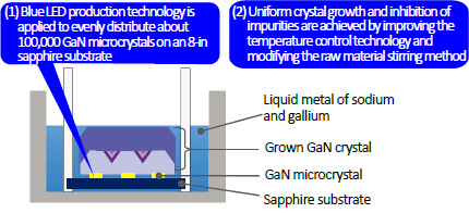
Toyoda Gosei and Osaka University have employed a method of growing GaN crystals in liquid metal of sodium and gallium (sodium flux method) to fabricate a high quality GaN substrate (GaN seed crystal) of over 6 inches (diameter 161 mm). They will next conduct quality assessments for mass production of 6-inch substrates, and continue improving quality and increasing diameter size (more than 6 inches).

