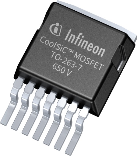
Infineon CoolSiC MOSFETs 650 V in D²PAK to Deliver Top Performance
The devices build on Infineon’s SiC trench technology and come in a compact D 2PAK SMD 7-pin package with .XT interconnection technology. They target high power applications including servers, telecom, industrial SMPS, fast EV charging, motor drives, solar energy systems, energy storage, and battery formation.
The new products offer improved switching behavior at higher currents and 80 percent lower reverse recovery charge (Q rr) and drain-source charge (Q oss) than the best silicon reference. The reduced switching losses allow high-frequency operations in smaller system sizes, enabling higher efficiency and power density. The trench technology is the basis for superior gate oxide reliability. Together with an improved avalanche and short-circuit robustness this ensures the highest system reliability even in harsh environments. The SiC MOSFETs are suitable for topologies with repetitive hard commutation as well as for high temperature and harsh operations. Thanks to a very low on-resistance (R DS(on)) dependency with temperature they show an excellent thermal behavior.
Featuring a wide voltage from gate to source (V GS) range from -5 V up to 23 V and supporting 0 V turn-off V GS and a gate-source threshold voltage (V GS(th)) greater than 4 V, the new family also works with standard MOSFET gate driver ICs. Additionally, the new products support bi-directional topologies and full dv/dt controllability, offering reduced system cost and complexity, as well as ease of adoption and integration. The .XT interconnection technology significantly improves the package’s thermal capabilities. Up to 30 percent extra loss can be dissipated compared to a standard interconnection.